Transistor and how to use it in the circuit
A transistor is a three-pin electronic component which its main function is to pass the current from two pins according to the other pin (along with current amplification). Transistors have different types, but we are going to examine the bipolar type here.
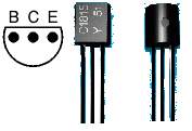
The two pins which the current passes are called the emitter (E) and the collector (C), and the pin that allows the current to pass is called the base (B). In the picture below, you can see the appearance of a common bipolar transistor but the arrangement of the pins may be different.
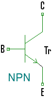
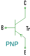
Bipolar transistors are divided into two categories: PNP and NPN.
The difference between these two categories is that the current input in PNP is from the emitter and the current output is from the collector, and the base controls the current output, but in NPN transistors, the current enters from the collector and exits from the emitter, and the base controls the current input.
The flat side of NPN transistors is black and sometimes PNP is silver (mostly try to identify the type of transistor from its name). There is the schema of these two types of transistors in the following.
In the following, the general operation of these two types of transistors and their related calculations are discussed.
- Examining the structure of the transistor is very complicated and requires information about quantum physics, and its overview cannot be understandable; So it is better to accept the transistor as it is for now.
NPN transistor and related calculations
As mentioned earlier, the current in this type of transistors enters to the collector and exits from the emitter (like its schema).
The base determines the maximum amount of the current that passes through the collector according to the current that enters it.
The maximum amount of current according to the following circuit is obtained from the following relationships
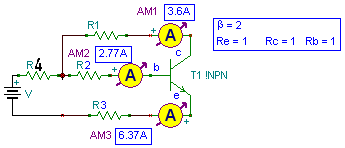
In the relations above, IB is the base current,
IC is the current passing through the collector,
IE is the emitter current,
RB is the base internal resistance,
RC is the collector-base resistance,
RE is the emitter-base resistance,
β is the coefficient between the current intensity of the base and the collector, which is also represented by hFE,
R is the resistance of the whole circuit,
R4 is the sum of the resistances before the place where the base and collector currents are separated and after the positive pole of the power supply (power input),
R1 is the sum of the resistances before the collector and after R4,
R2 is the sum of resistances before base and after R4,
and R3 is the sum of the resistors after the emitter.
- To calculate the resistance of the transistor, the resistance of the collector and base are considered in parallel and the result of these two resistances is considered in series with the emitter resistance.
You can control the collector input by changing the amount of R2, but the collector itself has no effect on the base input. By changing R3, both the input of the base and the input of the collector change.
When the collector is not working in the circuit, you can use the base-emitter as a diode.
- The β factor and resistances of the pins are defined in the transistor datasheet file. You can search the datasheet file with having the part number in Google.
The higher the voltage and current, decreases the calculation error percentage, because of the bias rates.
- Be careful that each transistor accepts only a limited current and voltage, otherwise it will be lost. You can find all these stated values from the datasheet file of the transistor.
PNP transistor and related calculations
In this type of transistors, the current enters to the emitter (as it can be seen from its schema) and exits from the collector.
The base determines the maximum amount of current that passes through the collector according to the current which is coming out of it.
The maximum amount of the current according to the following circuit is obtained from the following relationships
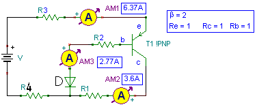
In the relations above, IB is the base current,
IE is the emitter current,
RB is the base resistance,
RC is the collector-base resistance,
RE is the emitter-base resistance,
β is the coefficient between base and collector current intensity (hFE),
R is the total resistance of the circuit,
R4 is the sum of the resistances before the place where the base and collector currents are separated and after the positive pole of the power supply,
R1 is the sum of the resistances before the collector and after R4,
R2 is the sum of resistances before base and after R4,
and R3 is the sum of the resistances after the emitter.
You can control the output of the collector by changing R2.
- The output of the collector has no effect on the output of the base and by changing R3, the output of the base and the collector both change.
- Diode D is used to prevent the current from entering to the base, because the return of the current to the base disrupts the output current from the collector and input to the emitter.
So far, all the work of a transistor has been examined. Think again about the effect of the pins on each other; Think carefully about formulas and ratios; This gives a complete understanding of the transistor to you. Understanding transistors is an introduction to understanding advanced electronics and digital.
Application of the transistor as an AND gate
An example of circuits that can be made by using transistors is the AND gate circuit. The AND gate is another digital logic gate, that if all the input currents are connected, the output current is connected.
The circuit below is the circuit of this gate which is made by two NPN transistors and one PNP transistor and has 2 inputs and 1 output.
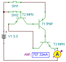
- the above schematic is designed only for the simulators.
The analysis of this circuit is as follows:
1) Both keys are off: It’s clear that the output (AM1) current will be zero.
2) Switch 1 (SW1) is connected and switch 2 (SW2) is disconnected:
In this case, the current enters from the positive side of the power supply to the circuit and after passing through SW1, it enters to the emitter of T1 and goes from the emitter to the base, but until the base current reaches the current output, the current does not exit through the collector.
When the base current of T1 reaches the collector of T2, because SW2 is off and no current reaches the base of T2, no current comes out of the emitter of T2.
Therefore the output will be zero.
3) SW1 is disconnected and SW2 is connected:
In this case, the current after passing through SW2 reaches the base of T2 and exits through the emitter of the same transistor and reaches the collector of T3, but since there is no current to enter to the base of T3, almost no current drains from the collector of T1 to the base of T3, so no current reaches to the output.
4) Both keys are connected:
The current enters from SW1, then goes to the emitter of T1. In T1, most of the current enters to the base and a very small amount (due to the presence of impurities in the materials of the transistor which is called the EC leakage) goes to its collector.
The base current of T1 goes to the collector of T2 and since SW2 is connected, the current entering the base and collector of T2 enters to the emitter of T2.
The current goes from the emitter of T2 to the collector of T3.
As a small amount of current drains into the base of T3 (at the first moment) through the collector of T1, the collector current of T3 exits through its emitter.
In the next moments, according to the hFE of the T1 transistor, the current leaves the collector of the same transistor and enters the base of T3, as the result, the current leaves the emitter of T3 and reaches to the output.
The true table of AND gate is in the following.
| SW1 | 0 | 1 | 0 | 1 |
| SW2 | 0 | 0 | 1 | 1 |
| output | 0 | 0 | 0 | 1 |
Transistor amplifiers
Here we are going to examine the three types of transistor amplifiers.
Earlier, we examined a type of current amplifier, and here there are the three types of amplifiers which can be made by using the transistors property:
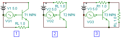
In the circuit number 1, RL is the consumer and is placed after the emitter.
According to the relationship between the currents and the structure of the transistor, the resistance of the consumer is effective in the input current to the base and the current accepted by the collector, so that we can conclude that the base current can be calculated by using the VG voltage and the resistance of the consumer.
- VG can be a circuit which produces a positive-wave signal (as we are using the NPN transistors in the examples).
The current can be calculated with multiplying the base current by hFE according to the acceptable current in the collector.
In the circuit number 2, the consumer is located before the collector and there is no resistor after the emitter, so in the calculation we consider only the production current in VG.
The best mode for the amplifier is this arrangement, because in this case, if the consumer resistance is variable, it will not take any effect on the base-emitter current.
In circuit number 3, as the base voltage of the transistor increases, the potential difference of the two ends of RL decreases.
- Be sure to pay attention to the characteristics of the transistor you are using and place the necessary resistors after the calculation before the collector or after the emitter.
- Check the gain ratio in these three types of amplifiers and also try to build these three types of amplifiers with PNP type transistor.
Flip-Flop
A flip-flop can commonly is a circuit which is consisting of two switches and two lamps, initially one of the lamps is on, and if we cut off the switch of that lamp, the other lamp turns on and stays on, even if the switch state changes again.
Since the method of using this operation by the transistor is important and is used in many cases, an example of a flip-flop by a transistor is as follows:
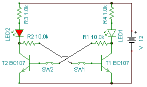
In the above flip-flop circuit, when the power is connected, one of the two LEDs will be on and the other one will be off. In the above circuit, LED2 is on. When you disconnect and connect the base of the transistor which its LED is on (which is connected and disconnected by SW2 in the circuit above), the LED of the other transistor will turn on and stay on, and if you do this again (this time with SW1) The same thing happens and the LED2 turns on, and the LED1 turns off.
The analysis of the above circuit is as follows:
The current from the positive pole of the power supply enters to the two resistors R3 and R4 and after passing through each LED, it is divided into two branches.
The current that enters R2 after LED2 goes to the base of T1 and causes the current of the collector of T1 to pass to the emitter and as a result, the current drains.
The current drains into the T2 in the same way. From this part, it is concluded that both LEDs turn on at the beginning, but both do not stay on, because according to the percentage of error that the resistors have, if the resistor connected to the base of one of the transistors is greater, causes to drain less current.
According to the input current, most of the current is drawn towards the base that has a lower resistance before it, and a very small current passes through the base of the other transistor; As the result, only one LED remains on.
If the current that enters to the base of the transistor which its LED is on is interrupted, the current goes to the base of the other transistor and is drawn to the other LED.
Now, if the switch is connected again, the LED will stay off because most of the current goes to the LED of the other transistor.
And the same thing, if SW2 is cut off, LED2 turns off and LED1 stays on, and because LED1 draws most of the current, we conclude that even when SW2 is closed again, LED2 does not turn on.
Frequency generation (oscillation)
To generate frequency in the direct current (e.g. VG circuit), we can use the property of the capacitor and transistor.
We first must know what “oscillation from direct current” means? As mentioned before, the diagram of DC signal is like a horizontal line, and the diagram of an AC signal is in the form of a wave. The act of generating frequency means to create an alternating signal by connecting and disconnecting the direct current repeatedly.
There are many ways to convert direct current to alternating current, one of which is the use of a relay, like “the single-LED flashing circuit” in the capacitor section.
We can use a multi-meter to measure the frequency (with help of an inductor to built sine wave). The multi-meter will measure the frequency according to the number of times that the voltage is increasing (the LED turns on) in one second.
The method of using the relay is too noisy, time-consuming, limited and inaccurate. Other methods of frequency generation are the use of the ICs and transistors. Here is a simple method using transistors to generate frequency.
One of the simplest ways to generate a frequency with a transistor is to use the flip-flop method.
Flip-flop oscillator
If we connect a multi-meter (in frequency mode and with help of an inductor) to the two pins of the LED in the circuit below, it will show the frequency as the number of times the LED turns on in one second:
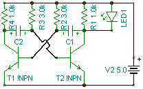
When the frequency is high (e.g. 10Hz) the LED seems constantly turned on. The frequency in this circuit depends on the R2 and R3, the lower these resistors increase the frequency.
In practice, if we use 0.33 uF capacitors and 4.7K resistors for R1 and R4, and 47K for R2 and R3 and C945 transistors, the circuit can produce about 650Hz of frequency.
The best way to precisely adjust the frequency is to use an IC, which we will discuss in the following articles.
Transistor circuit examples
Two-LEDs flashing circuit:
Required equipment: two 1KΩ resistors, two 33KΩ resistors, two 56μF capacitors, two BC107 transistors, two LEDs, 12V power supply.
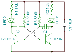
If you make this circuit according to the schematic plan, you will see that one LED turns on and and after about 1 second it turns off and the other LED turns on and it repeats.
Circuit analysis:
The above circuit is made by using flip-flop method. After the current enters to the circuit, an LED turns on and stays on until the capacitor which is connected to the base of the LED’s transistor is enough charged. Then the LED turns off because its transistor’s base doesn’t receive enough bias current.
Therefore the other LED turns on until its capacitor is charging and the other capacitor is discharging. R3 and R4 resistors are used to discharge the charged capacitors.
Reverse gate (Inverter):
The schematic below shows the inverter circuit:
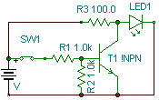
The “Inverter” is another digital logic gate.
If SW1 is closed, LED1 will turn off, otherwise it will be turned on.

Written by: M. Mahdi K. Kanan – Full stack electronics and programming engineer and the founder of WiCardTech