Circuit design and construction
You must have realized what electronic circuit means during your life. In general, we can have this definition of an electronic circuit:
A set of parts which their pins are connected in a special way with a conductive material (such as copper) to each other and they are supposed to make changes to the incoming current or power.
- In a correct circuit, it is possible to entering and exiting the current to each of the parts.
The circuit schematic plan
A map or plan that specifies how parts are connected to each other is called a schematic map.
It is better to draw this plan with a computer software, so it can be easily edited in case of any problems.
Some software or applications have a circuit simulator or test programs.
Every electronic component or part has its own schema or symbols used in the schematic plan which shows an approximate form of the internal structure of the part or its function. In this way, the type of parts used can be understood by everyone.
To analyze a schematic, it is best to start with the main input current from the power supply.
- Try to analyze some simple schematics and check the correctness of your analysis practically or by using simulator software.
The symbols in a circuit schematic map
First of all, try to draw an outline in your mind of how the parts should be connected.
It is up to you when to start drawing the schematic, but it is better to first build the blocks/sections of the circuit that you are not completely sure of the correctness of the image in your mind with a simulation software or on a breadboard..
After arrangmenting all of the blocks in your mind, start drawing the overall schematic using the software.
In the drawing, the technical schema of the parts (symbol) is used to show them, and each part must have a designator name e.g. R1, R2 etc.
It is enough to arrange the parts and connect the branches which is marked as the pin of the part with a line, as necessary.
Here are some of the part’s schema and designator (depending on your software, may be different):
Resistor (R):

Potentiometer (variable resistor) (P, R or VR):

Non-polarized capacitor (C):

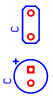
Polarized capacitor (C):

Variable capacitor (VC):

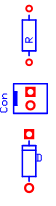
Battery or power supply (P, B or Con):

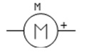
Electric motor (M):
A typical diode (D):

Light emitting diode (L, D or LED):

Zener diode (Z, D):

Microphone (Mic):

Speaker (Sp):

Inductor/Coil (L):

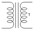
Transformer (T):
- In the schematic drawing, one or more currents are always entered (through the battery, power supply or other circuits) and the necessary processing is done in the circuit on this current and it may have one or more outputs.
Draw a node in the circuit diagram
A node is a point where at least two track lines are connected to each other. This point must be bold enough to separate from the crossed tracks which are not connected.
- Sometime we do now draw the grand track (Negative pole of the power supply) and use the ground symbol instead to simplify the schematics.
- It is better to draw the shortest track lines as possible.
Drawing the circuit’s schematic map
To draw the circuit schematic, you need pay attention to the following tips:
- Use of 1 diode to prevent incorrect input current.
- By using a capacitor in parallel (a filter/decoupling capacitor) avoid the noises or sudden power fluctuations. The capacity of this capacitor should be adjusted according to the input voltage.
- It is better to put a diode between the two legs of the relay coil pins, because this diode causes to avoid inductance noises.
- In the areas where several track lines go to an output track, using the diodes can prevent the reverse current.
- You can calculate the required input voltage/current by using the needed formulas.
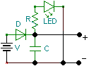
The following schematic diagram shows an example of a protector block of a circuit:
It is very important to follow the tips when you are going to use an IC.
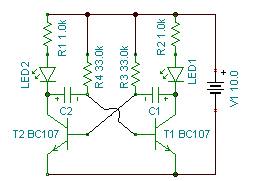
The following picture shows the schematic diagram of a two-LEDs flasher:
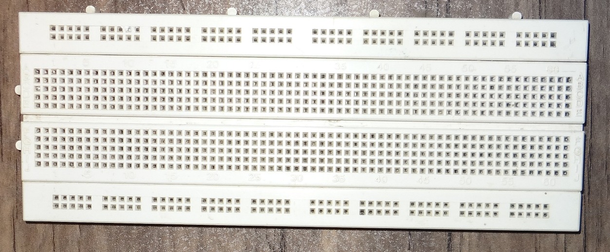
The Circuit on a Breadboard
A breadboard is a platform that is used for testing circuits before designing its printed circuit board (PCB).
There are so many holes on the breadboard and they are connected in groups (usually 5 groups).
The size of the holes is the same as the pins of the parts, and it does not need to be soldered.
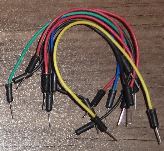
Breadboard wires:
Printed circuit board (PCB) drawing
The map or plan which is using for the PCB is different from the schematic map. In a PCB plan, an image that shows the location of the pins on the board in their real size is using instead of using the part’s schema or symbol.
A PCB drawing has three main parts:
The top side routes and holes (top layer-for two-way boards)
The bottom side routes and holes (bottom layer)
The components guide layer (silk screen)
Double-sided board: A board that has both of top layer and bottom layer.
Metallized board: a double-sided board which the upper holes lead to the lower holes. (A very thin layer of a conductive material connects the top of the holes to the bottom)
The silkscreen is a shadow of the part on the board and also shows the part name and number.
For example, two holes for the pins, with a suitable distance and a rectangle in the silkscreen is using for a resistor. For the diode, a rectangle with a line inside and for a capacitor, a circle.
Foot print of some of the parts on the PCB (in order: resistor, connector, diode, capacitor, polarized capacitor):
Drawing the circuit’s PCB plan
To draw a PCB design, it is better to try to use the known PCB design software.
- Before starting the PCB design, draw the schematic and add it to your PCB file.
Usually, there are the most used parts/components in the software’s library with their standard size.
After placing the desired parts, you must connect the pins of the parts with using Tracks/Traces (conductive paths) or the software auto-route.
Pay attention that for better printing of the routes, they should not have an angle other than 45 degrees and 135 degrees.
Example of the correct paths:


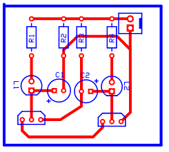
The PCB design of two-LEDs flasher which is designed with software:
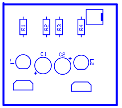
The silkscreen:
The bottom layer:
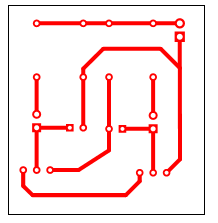
- The location of the holes is indicated in the bottom layer.
- Use a jumper (a piece of wire) with adding two holes if two routes must cross on each other without connection.
- For complex circuits with many connections, you can use double-sided or metallized printed circuit board.
The circuit’s bill of material (BOM)
Using a table that contains the name of the part, its number and its code/serial or value is necessary when you are going to assemble the board. This table is called BOM (Bill Of Materials).
For example, the table below is for a two-LEDs flasher:
| Designator | Serial/Value |
| T1,T2 | BC107 |
| R1,R2 | 1 K |
| R3,R4 | 33 K |
| LED1 | 5mm Red |
| LED2 | 5mm Green |
| C1,C2 | 56uF |
Assembling the circuit’s board
Place the parts/components on the printed board according to the silkscreen and BOM. Solder the part first and then cut the part’s extra ends/wires

Written by: M. Mahdi K. Kanan – Full stack electronics and programming engineer and the founder of WiCardTech