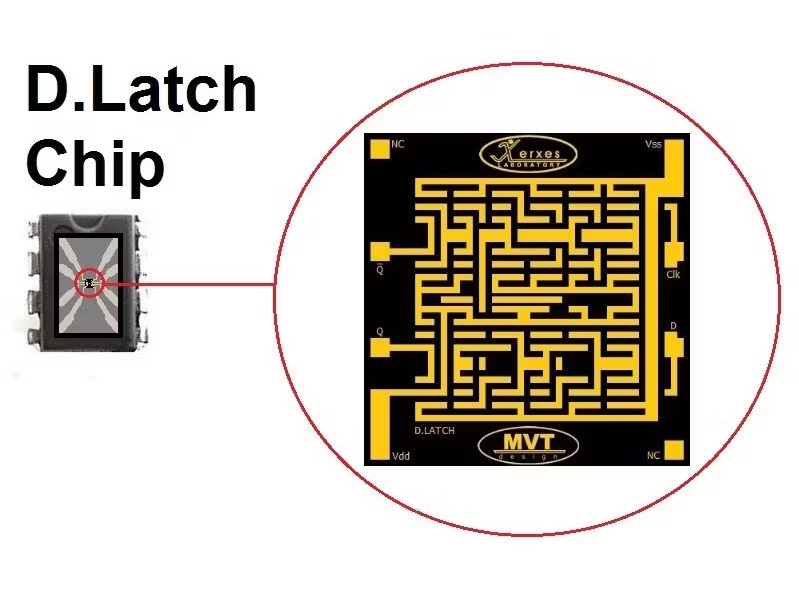
D Latch Flip-Flop Chip Design
A D Latch flip flop is in fact a one bit “Random Access Memory (RAM)”. That means at the start up, “Q” pin may be “1” or “0”. With paralleling 8 of D. Latches, you can make an 8-bit or one byte RAM.
The D Latch that I had designed on a paper is a bit different than usual schematics. When I designed it, I was only 20 and designed it by reading some articles about digital gates and integrated circuits design.
The D Latch Flip Flop Schematics
Here’s the schematics:
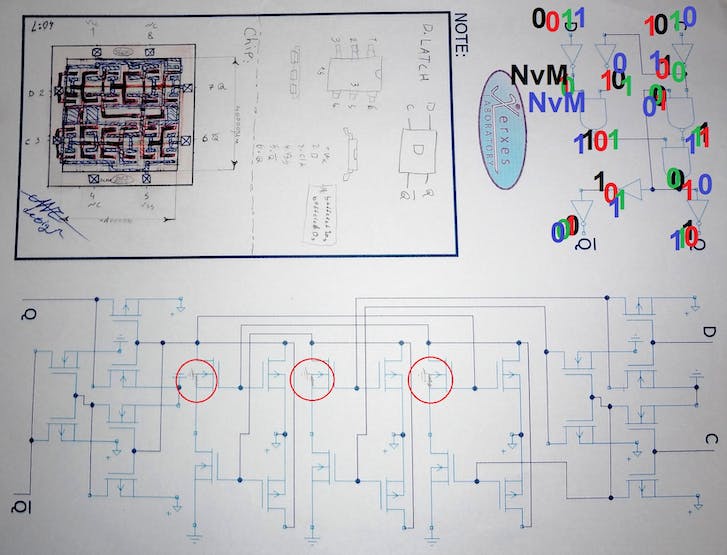
In that time I was really interested in CPU designing (and still I am), it was a good start but only just. Sometimes I don’t believe that it had designed by me when I was only 20, because everything exactly on it’s place, even I noticed to MOSFETs “substrates connections”.
Right now I’ve noticed that the outputs and inputs are buffered and in usual D. Latches they used 26 MOSFETs, but I’ve used 24 MOSFETs.
Anyway, a one bit ram takes 24 MOSFETs, a one byte takes 24*8 and a one kilo bytes ram has 196608 MOSFETs inside of it.
In my designed flip-flop, when the “clk” pin is “0”, “D” pin doesn’t any effect on the “Q” pin. When “clk” is logically “1”, the “Q” shows the logical data on “D”.
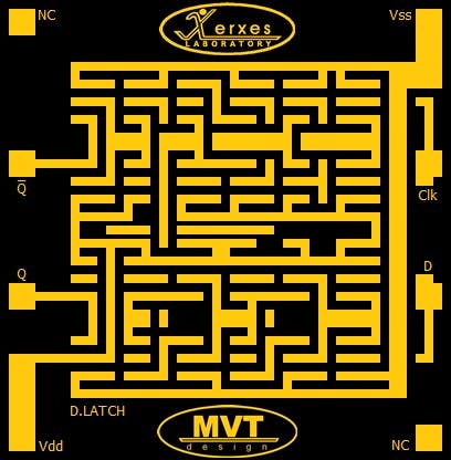
Chip Layers
I considered 3 main layers for the chip. On every layers some tracks and P and N materials must be implanted and etched.
The first layer: MOSFETs
The Second Layer: Bottom Tracks
The Third Layer: Top Tracks
This is a P-Type wafer and the main substrate for the N-Channel MOSFETs:

The first step is implanting N-Type substrate inside of the P-Type wafer:

The second step is implanting Active P-Type (P+) semiconductors on the chip:
The third step is implanting Active N-Type (N+) semiconductors on the chip:
The fourth step is etching the Oxides on the MOSFETs gate:
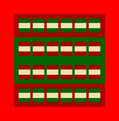
Now, 24 MOSFETs has been implanted on the chip.
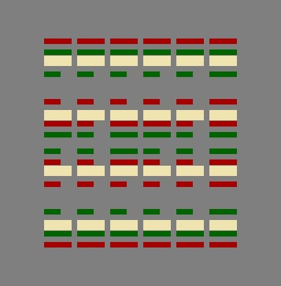
The fifth step is covering the chip with a “Dielectric layer”:
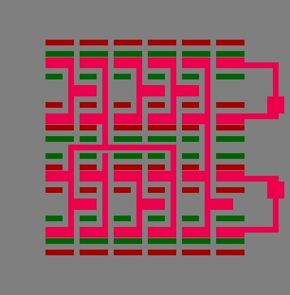
the sixth step is etching Poly layer (e.g. PolySi) as the bottom track layer:
The seventh step is covering the bottom layer with another dielectric layer:
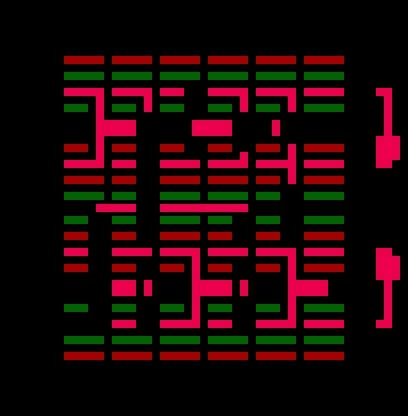
And the eighth step is etching the tracks and input/output pins on the chip:
The processes

The D Latch Flip Flop Truth Table
// D. Latch Flip Flop Truth Table
// CLK| D | Q |~Q
// ---------------
//  0 | 0 | L | L
//  0 | 1 | L | L
//  1 | 0 | 0 | 1
//  1 | 1 | 1 | 0
Written by: M. Mahdi K. Kanan – Full stack electronics and programming engineer and the founder of WiCardTech