Operational Amplifier IC (OP-AMP)
Operational Amplifier ICs (Op-Amp ICs) are usable for amplifying weaker voltages and currents.
For example, the output of a signal generator with is a current of 10 micro-amps with 3 volts oscillation, but our circuit needs a 3 volts signal with a 3 milli-amps current. With using an operational amplifier, we provide the required current while we do not need to make changes in the signal voltage.
Operational amplifier IC structure
In the previous articles, I introduced the ICs (integrated circuits), and here I’m going to talk about the internal structure/circuit of LM741 OP-Amp IC.
The performance of other operational amplifier ICs is generally the same.
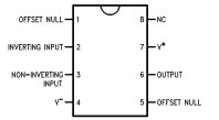
We start with the pin order of this IC:
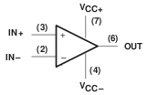
The schematic diagram of this operational amplifier is shown in the following:
Pin 8 is NC that means should not be connected anywhere. Pin 1 is the offset pin which generally we do not need this pin.
Also in the simplified/conceptual schematics there’s no need to draw power supply pins (4 and 7).
The main duty of this IC is to perform mathematical operations on the signals, but due to the interesting properties of this IC, it can also be used as an oscillator.
The IC pins
7 (Vcc+) and 4 (Vcc-/Vss/GND): These pins are related to IC power supply. The best voltage for LM741 is between 9V to 20V.
3 (IN+): The input voltage of this pin will exit from the output pin with the same phase. This input pin is also called “The same phase input”.
2 (IN-): The input voltage of this pin will exit from the output pin with the reverse phase. This input pin is also called “The phase shifter input”.
6 (Output): The result of the signal applying in the other pins, appears here.
Now let’s examine the schematic of the internal circuit of this IC:
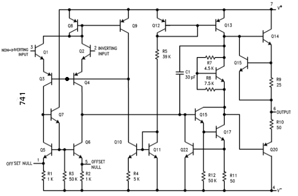
After analyzing the circuit above (be sure to do this), you will find that if pin 2 is off, pin 3 has no role in the output.
If the IC is powered, pin 2 will reduce the IC’s preset output.
The role of pin 3 is only to send the input voltage from pin 2 to the output, which causes the output which was reduced to increase.
If the IC be perfectly balanced, if the input voltages be equal, the output will be the same voltage as when no pin is connected.
To better understanding this, try different voltages on the inputs and measure and output voltage of an LM741CN IC with a multi-meter.
AC signals and the operational amplifier
Suppose 2V is passing on a route and we reduce it by half with this IC, now we have 1V output. If the input becomes 3 volts, the output will be 1.5 volts.
In the alternating signal, it is the same.
If our goal is to amplify a signal, all its points are multiplied by the amplification factor and will be revealed in the output.
Mathematical operations on voltages are performed by the operational amplifier IC.
feedback
Feedback is a situation when one of the input pins of the component is fed by its output.
For example, in an operational amplifier, connect the output pin to the phase shifter input (either directly or with a resistor).
By using feedback, you can reach a logic about the voltage between the pins, which one of the feedback arrangements is in the following circuit:
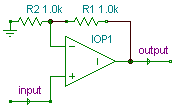
Gain = 1 + R1/R2
Obviously, if the input voltage of the phase shifter is reduced, the effect of voltage amplification will be also reduced, and if its current is reduced, the voltage amplification will be very high due to the high resistance of the input pin.
The mathematical circuits such as adder, multiplier, subtracter, integrator, derivative and many other circuits can be made by using this property.
Voltage follower (buffer)
If R1 be 0 ohms (short circuit) and we remove R2, the result circuit is called the voltage follower.
In this case, the output voltage will be equal to the input voltage, but the current will be amplified.
- The most important characteristic of the output of the operational amplifier IC in this case is its current stability, if the input becomes weak, the output remains almost constant.
Filters
If you put a 330 ohm resistor after LM741CN, you can consider the output resistance 1000 ohms, and if the resistance after the IC is more than 3300 ohms, the output resistance of the IC is equal to the same amount of resistors after the IC.
The OP-Amp simplified the calculations. Also you can use a transistor amplifier for easier calculation.
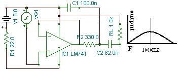
The above circuit is a mid-pass filter circuit that is set to 1000 Hz frequency and is made with the current amplification feature of this IC.
It is better to use a load resistor for the positive input of the IC.
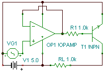
Signal amplifier circuit
In the following circuit, the generated signal current in VG1 is amplified:

Written by: M. Mahdi K. Kanan – Full stack electronics and programming engineer and the founder of WiCardTech